

Mail: sales@lonstarpcb.com / sales@lonstarpcba.com
High-Quality-PCBA-Manufacturing-Process
Source:
|
Author:Lonstar
|
Published time: 779 days ago
|
451 Views
|
🔊 Click to read aloud
❚❚
▶
|
Share:
The PCBA production process can be divided into several major processes, SMT surface mount processing → DIP Soldering processing → PCBA testing →coating → finished product assembly.
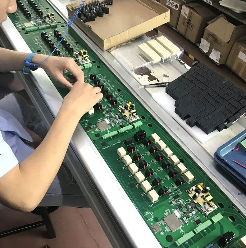
1. SMT components placement processing process
The process of SMT surface mount processing is as follows: solder paste stirring → solder paste printing → SPI → components mounting → reflow soldering → AOI → repair
⓵ Solder paste stirring
After thawing the solder paste from the refrigerator, use manual or machine stirring to make it suitable for printing and welding.
⓶ Solder paste printing
Place the solder paste on the steel mesh and use a scraper to leak the solder paste onto the PCB pad.
⓷ SPI
SPI, also known as solder paste thickness detector, can detect the printing situation of solder paste and control the printing effect of solder paste.
⓸ Installation
The SMT components are placed on the Feida, and the SMT machine head accurately attaches the components on the Feida onto the PCB pads through recognition.
⓹ Reflow soldering
The PCB board is reflow soldered, and the high-temperature inside causes the paste like solder paste to heat up and become liquid. Finally, it cools and solidifies to complete the soldering.
⓺ AOI
AOI stands for automatic optical detection, which can detect the NG soldering of PCB boards by scanning, and detect defects in the boards.
⓻ Repair
Repair the defects detected by AOI or manual inspection.
2. DIP plugin processing stage
The process of DIP plugin processing is as follows: plugin → wave soldering → foot cutting → post welding processing → plate washing → quality inspection
⓵ Plug in
Process the pins of the plug-in materials and insert them onto the PCB board
⓶ Wave soldering
Pass the inserted board through the wave soldering process, during which liquid tin is sprayed onto the PCB board, and finally cool down to complete the soldering.
⓷ Cutting feet
The pins of the welded board are too long and need to be trimmed.
⓸ Post soldering processing
Use an electric soldering iron to manually solder components.
⓹ Wash and clean board
After wave soldering, the boards will be quite dirty and need to be cleaned with plate washing water and tank, or by machine.
⓺ Quality inspection
Inspect the PCB board. Unqualified products need to be repaired before they can proceed to the next process.
3.PCBA testing
PCBA testing can be divided into ICT testing, FCT testing, aging testing, vibration testing, etc
PCBA testing is a large-scale test, and the testing methods used vary depending on different products and customer requirements. ICT testing is to detect the soldering of components and the continuity of circuits, while FCT testing is to test the input and output parameters of the PCBA board to see if they meet the requirements.
4. PCBA coating
The PCBA proof coating process steps are: brushing surface A → surface drying → brushing surface B → room temperature curing. 5. Spray thickness: Spray thickness: 0.1mm-0.3mm. 6. All coating operations should be carried out under conditions of no less than 16 ℃ and relative humidity below 75%.
PCBA proof coating is still widely used, especially in environments with harsh temperature and humidity. PCBA coated three proof paint has superior insulation, moisture resistance, leakage resistance, shock resistance, dust prevention, corrosion resistance, aging resistance, mold resistance, anti loosening of parts, and insulation resistance to corona, which can extend the storage time of PCBA, isolate external corrosion, pollution, etc. The spraying method is the most commonly used coating method in the industry.
5. Finished product assembly
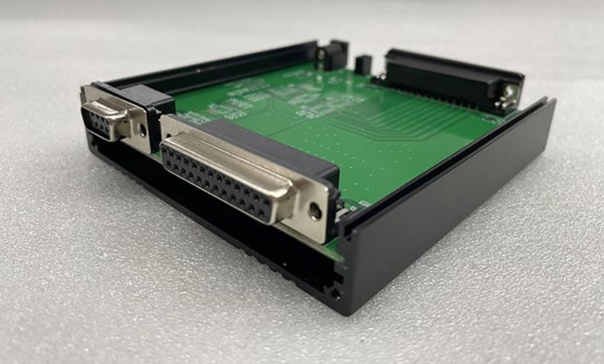
The PCBA board that has been coated and tested OK will be assembled into the case, then tested, and finally shipped.
PCBA production is a process of interlocking links, and any problem in any link will have a significant impact on the overall quality. Strict quality control is required for each process.
Prev:
None
QUICK LINK


SHIPPING METHODS
CONTACT US


LEAVE A MESSAGE


Link
