Foreign markets also look at the smt processing industryvery much. The four major driving forces, 5G networks, as well as the cloud,automobiles and new-generation mobile devices, are about to become the mainservice targets.
HDI board (High Density Interconnector), namely high-density interconnection board, is a circuit board with high circuit distribution density using micro blind hole embedding technology. The HDI board has an inner layer circuit and an outer layer circuit, and then uses drilling, hole metallization and other processes to connect the internal circuits of each layer.
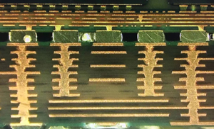
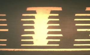
HDI holes are not mechanically drilled. The aperture of micro blind holes is less than or equal to 150um (6mil). The L/S of internal and external layer tracks is less than 4mil, and the pad diameter is ≤ φ 0.35 mm they are designed and manufactured based on these parameter.
1、Product features
a. The lines are relatively dense;
b. More laminate pressing procedures;
c. High requirements for inter layer alignment;
d. More BGA;
e. Laser blind hole;
f. The drilling hole density is high and the hole diameter is small;
g. Hole filling by electroplating (some HDI PCB only need common electroplating, only plate blind hole wall);
h. The solder mask bridge is small;
2、 Product difficulties
a. Product inflation control;
b. Laminate pressing of each compression;
C. Alignment between layers;
d. Quality control of blind hole type and hole bottom;
e. Copper backlight control;
f. Hole filling quality;
g. Fabrication of outer tracks;
h. Solder mask quality (deviation and bridge peel off);